- 您现在的位置:买卖IC网 > Sheet目录2008 > MAX1183ECM+TD (Maxim Integrated Products)IC ADC 10BIT 40MSPS DL 48-TQFP
component is 90 degree phase-shifted with respect to
the in-phase component. At the receiver, the QAM signal
is divided down into its I and Q components, essentially
representing the modulation process reversed. Figure 8
displays the demodulation process performed in the
analog domain, using the dual matched 3V, 10-bit ADC
(MAX1183), and the MAX2451 quadrature demodulator
to recover and digitize the I and Q baseband signals.
Before being digitized by the MAX1183, the mixed-down
signal components may be filtered by matched analog
filters, such as Nyquist or pulse-shaping filters, which
remove any unwanted images from the mixing process,
thereby enhancing the overall signal-to-noise (SNR) per-
formance and minimizing intersymbol interference.
Grounding, Bypassing, and
Board Layout
The MAX1183 requires high-speed board layout design
techniques. Locate all bypass capacitors as close to
the device as possible, preferably on the same side as
the ADC, using surface-mount devices for minimum
inductance. Bypass VDD, REFP, REFN, and COM with
two parallel 0.1F ceramic capacitors and a 2.2F
bipolar capacitor to GND. Follow the same rules to
bypass the digital supply (OVDD) to OGND. Multilayer
boards with separated ground and power planes pro-
duce the highest level of signal integrity. Consider the
use of a split ground plane arranged to match the
physical location of the analog ground (GND) and the
digital output driver ground (OGND) on the ADC’s
package. The two ground planes should be joined at a
single point such that the noisy digital ground currents
do not interfere with the analog ground plane. The ideal
location of this connection can be determined experi-
mentally at a point along the gap between the two
ground planes, which produces optimum results. Make
this connection with a low-value, surface-mount resistor
MAX1183
Dual 10-Bit, 40Msps, 3V, Low-Power ADC with
Internal Reference and Parallel Outputs
______________________________________________________________________________________
15
MAX1183
T1
N.C.
VIN
6
1
5
2
4
3
22pF
0.1F
2.2F
25
MINICIRCUITS
TT1–6
T1
N.C.
VIN
6
1
5
2
4
3
22pF
0.1F
2.2F
25
MINICIRCUITS
TT1–6
INA-
INA+
INB-
INB+
COM
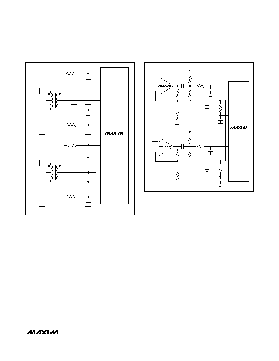
Figure 6. Transformer-Coupled Input Drive
MAX1183
0.1F
1k
100
CIN
22pF
CIN
22pF
INB+
INB-
COM
INA+
INA-
0.1F
RISO
50
RISO
50
REFP
REFN
VIN
MAX4108
0.1F
1k
100
CIN
22pF
CIN
22pF
0.1F
RISO
50
RISO
50
REFP
REFN
VIN
MAX4108
Figure 7. Using an Op Amp for Single-Ended, AC-Coupled
Input Drive
发布紧急采购,3分钟左右您将得到回复。
相关PDF资料
MAX1184ECM+TD
IC ADC 10BIT 20MSPS DL 48-TQFP
MAX1186ECM+TD
IC ADC 10BIT 40MSPS DL 48-TQFP
MAX1187CCUI+
IC ADC 16BIT 135KSPS 28-TSSOP
MAX118EAI+
IC ADC 8BIT 1MSPS 28-SSOP
MAX1191ETI+T
IC ADC 8BIT 7.5MSPS DL 28-TQFN
MAX1192ETI+T
IC ADC 8BIT 22MSPS DL 28-TQFN
MAX1195ECM+TD
IC ADC 8BIT 40MSPS DL 48-TQFP
MAX1197ECM+TD
IC ADC 8BIT 60MSPS DL 48-TQFP
相关代理商/技术参数
MAX1183ECM-D
功能描述:模数转换器 - ADC RoHS:否 制造商:Texas Instruments 通道数量:2 结构:Sigma-Delta 转换速率:125 SPs to 8 KSPs 分辨率:24 bit 输入类型:Differential 信噪比:107 dB 接口类型:SPI 工作电源电压:1.7 V to 3.6 V, 2.7 V to 5.25 V 最大工作温度:+ 85 C 安装风格:SMD/SMT 封装 / 箱体:VQFN-32
MAX1183ECM-TD
功能描述:模数转换器 - ADC RoHS:否 制造商:Texas Instruments 通道数量:2 结构:Sigma-Delta 转换速率:125 SPs to 8 KSPs 分辨率:24 bit 输入类型:Differential 信噪比:107 dB 接口类型:SPI 工作电源电压:1.7 V to 3.6 V, 2.7 V to 5.25 V 最大工作温度:+ 85 C 安装风格:SMD/SMT 封装 / 箱体:VQFN-32
MAX1184ECM
制造商:Maxim Integrated Products 功能描述:DUAL 10-BIT, 20MSPS, +3V, LOW-POWER ADC WITH - Rail/Tube
MAX1184ECM+D
功能描述:模数转换器 - ADC 10-Bit 2Ch 30Msps High Speed ADC RoHS:否 制造商:Texas Instruments 通道数量:2 结构:Sigma-Delta 转换速率:125 SPs to 8 KSPs 分辨率:24 bit 输入类型:Differential 信噪比:107 dB 接口类型:SPI 工作电源电压:1.7 V to 3.6 V, 2.7 V to 5.25 V 最大工作温度:+ 85 C 安装风格:SMD/SMT 封装 / 箱体:VQFN-32
MAX1184ECM+TD
功能描述:模数转换器 - ADC 10-Bit 2Ch 30Msps High Speed ADC RoHS:否 制造商:Texas Instruments 通道数量:2 结构:Sigma-Delta 转换速率:125 SPs to 8 KSPs 分辨率:24 bit 输入类型:Differential 信噪比:107 dB 接口类型:SPI 工作电源电压:1.7 V to 3.6 V, 2.7 V to 5.25 V 最大工作温度:+ 85 C 安装风格:SMD/SMT 封装 / 箱体:VQFN-32
MAX1184ECM-D
功能描述:模数转换器 - ADC RoHS:否 制造商:Texas Instruments 通道数量:2 结构:Sigma-Delta 转换速率:125 SPs to 8 KSPs 分辨率:24 bit 输入类型:Differential 信噪比:107 dB 接口类型:SPI 工作电源电压:1.7 V to 3.6 V, 2.7 V to 5.25 V 最大工作温度:+ 85 C 安装风格:SMD/SMT 封装 / 箱体:VQFN-32
MAX1184ECM-T
制造商:Maxim Integrated Products 功能描述:DUAL 10-BIT, 20MSPS, +3V, LOW-POWER ADC WITH - Tape and Reel
MAX1184ECM-TD
功能描述:模数转换器 - ADC RoHS:否 制造商:Texas Instruments 通道数量:2 结构:Sigma-Delta 转换速率:125 SPs to 8 KSPs 分辨率:24 bit 输入类型:Differential 信噪比:107 dB 接口类型:SPI 工作电源电压:1.7 V to 3.6 V, 2.7 V to 5.25 V 最大工作温度:+ 85 C 安装风格:SMD/SMT 封装 / 箱体:VQFN-32